3D printed multilayer structures for high-numerical aperture achromatic lenses

This article has been reviewed according to Science X’s editorial process
and policies.
Editors have highlighted the following attributes while ensuring the content’s credibility:

fact-checked

peer-reviewed publication

trusted source

proofread


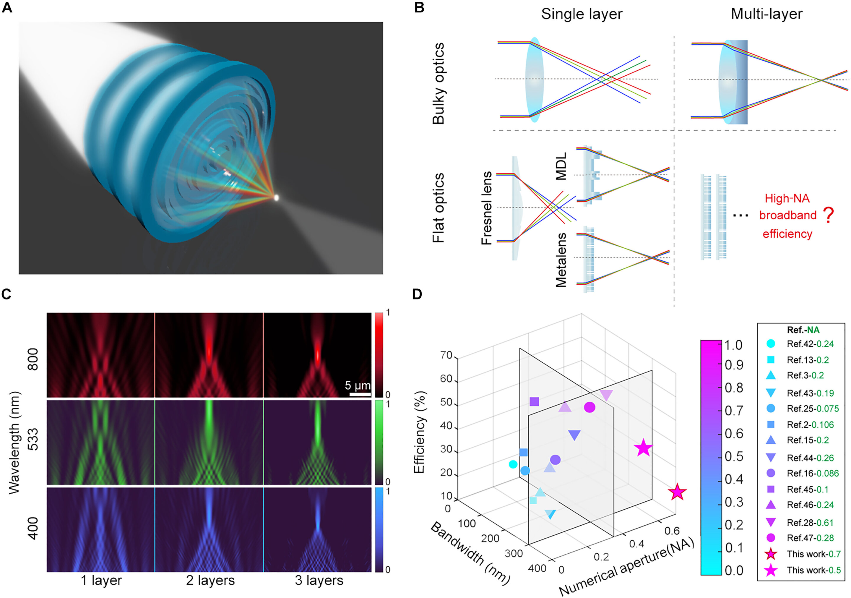
Achromatic performance of different single lenses and multilayer lenses. (A) Schematic of the designer 3D-printed multilayer achromatic metalens (MAM). (B) Schematic of traditional and flat optics lenses [including Fresnel lens, multilevel diffractive lens (MDL), and metalens] with single layers and multilayers. (C) Evolution of focal spots at wavelengths of 400, 533, and 800 nm when additional layers are added (results are from an optimized three-layer design of 0.5-NA MAM). (D) The efficiencies, numerical apertures, and bandwidths (works in the visible band) of various achromatic metalenses. The color bar and marker size represent the figure or merit defined as the square root of the sum of squares of efficiency, NA, and bandwidth. The gray planes indicate previous limits at bandwidth = 300 nm and NA = 0.35. The NA values of each metalens are illustrated in the legend. Credit: Science Advances, doi: 10.1126/sciadv.adj9262

× close


Achromatic performance of different single lenses and multilayer lenses. (A) Schematic of the designer 3D-printed multilayer achromatic metalens (MAM). (B) Schematic of traditional and flat optics lenses [including Fresnel lens, multilevel diffractive lens (MDL), and metalens] with single layers and multilayers. (C) Evolution of focal spots at wavelengths of 400, 533, and 800 nm when additional layers are added (results are from an optimized three-layer design of 0.5-NA MAM). (D) The efficiencies, numerical apertures, and bandwidths (works in the visible band) of various achromatic metalenses. The color bar and marker size represent the figure or merit defined as the square root of the sum of squares of efficiency, NA, and bandwidth. The gray planes indicate previous limits at bandwidth = 300 nm and NA = 0.35. The NA values of each metalens are illustrated in the legend. Credit: Science Advances, doi: 10.1126/sciadv.adj9262

Flat optics are made of nanostructures containing high-refractive index materials to produce lenses with thin form factors that function only at specific wavelengths.

Materials scientists have recently attempted to achieve achromatic lenses to uncover a tradeoff between the numerical aperture and bandwidth that limits the performance of such materials. In this work, Cheng-Feng Pan and a team of scientists in engineering product development, information technology, and computer engineering in Singapore and China proposed a new approach to design high numerical aperture, broadband, and polarization-insensitive multilayer achromatic metalenses.

The materials scientists combined topology optimization and full wavelength simulations to inversely design the metalenses using two-photon lithography. The research team demonstrated the broadband imaging performance of the engineered structures under white light and red, green, and blue narrowband illuminations.

The outcomes highlighted the capacity of the 3D-printed multilayer structures to realize broadband and multifunctional meta devices. The outcomes are now published on Science Advances and are featured on the cover page of the journal.

Imaging performance

Recent progress in metalenses at the micro- and macro-scale have shown significance to achieve remarkable imaging performance suited for a variety of applications across light-field imaging, bioanalysis, medicine, and quantum technologies. For instance, achromatic lenses show broadband responses to capture color information, to expand the design possibilities and application scenarios for photonic devices.

Such constructs are ultra-compact, ultra-thin, light-weight, and well-suited to make compelling metalenses for imaging systems. Most metalenses are, however, patterned in high refractive index materials to provide good optical control, with a strong light that makes broadband implementation challenging.

Physicists have shown the Abbe number as a figure of merit in lens design to represent a dispersion-free transparent material commonly used for high-refractive index materials and as a formula to realize a high-efficiency focusing lens.


Topology optimization of the MAM with different layer number and spacing distance. (A) Design model and schematic of the optimization region with indicated parameters described in the text. (B) Relations of the normalized intensity with the layer number and spacing distance. With the inverse design, the best case is located at [l, sp] = [3, 1.6 μm]. (C) Schematic of the edge rounding and surface smoothness approximations at different levels, initial design (i), level 1 by rounding the top (ii). Level 2 is generated by applying 10-nm relative tolerance interpolation to the origin height vector (iii), and level 3 is generated by applying 25-nm relative interpolation (iv). (D) Calculated FWHM (i), efficiency (ii), and position of maximum focal intensity along the propagation axis (iii) for different levels. The efficiency (ii) is calculated at the focal plane corresponding to the maximum focal intensity. (E) Tilted view SEM images of the fabricated MAM with 0.5 NA: (i) deconstructed MAM showing single, double, and triple (full) layers; (ii) enlarged view of full MAM; (iii) top view and size of the MAM; and (iv and v) sectioned MAM revealing internal structure and details of the 200-nm-wide ring structures. Credit: Science Advances, doi: 10.1126/sciadv.adj9262

× close


Topology optimization of the MAM with different layer number and spacing distance. (A) Design model and schematic of the optimization region with indicated parameters described in the text. (B) Relations of the normalized intensity with the layer number and spacing distance. With the inverse design, the best case is located at [l, sp] = [3, 1.6 μm]. (C) Schematic of the edge rounding and surface smoothness approximations at different levels, initial design (i), level 1 by rounding the top (ii). Level 2 is generated by applying 10-nm relative tolerance interpolation to the origin height vector (iii), and level 3 is generated by applying 25-nm relative interpolation (iv). (D) Calculated FWHM (i), efficiency (ii), and position of maximum focal intensity along the propagation axis (iii) for different levels. The efficiency (ii) is calculated at the focal plane corresponding to the maximum focal intensity. (E) Tilted view SEM images of the fabricated MAM with 0.5 NA: (i) deconstructed MAM showing single, double, and triple (full) layers; (ii) enlarged view of full MAM; (iii) top view and size of the MAM; and (iv and v) sectioned MAM revealing internal structure and details of the 200-nm-wide ring structures. Credit: Science Advances, doi: 10.1126/sciadv.adj9262

The 3D printing method

The research team lifted the fabrication challenges underlying multilayer achromatic metalenses by using three-dimensional printing. The nanoscale 3D printing method allowed the patterning of a multilayer lens in one lithographic step to rapidly prototype complex structures. Using two-photon polymerization, the scientists realized a variety of 3D designs, including complex microlenses, gradient index lenses, and diffractive lenses.

In this work, Pan and colleagues used topology optimization to achieve achromatic lensing behavior. They achieved a stable, multilayer, and high-resolution structure quickly.

The resulting multilayer achromatic metalenses showed hitherto unknown levels of efficient performance to integrate the advantages of nanoscale high-resolution 3D printing to create metalenses with exceptional performance to inspire a new paradigm to design and fabricate multifunctional broadband optical elements and devices.

Designing multilayer achromatic metalenses and the experimental outcomes


Focusing efficiency and imaging performance of MAM. (A) Comparison of experiment and simulated broadband focusing efficiencies for MAMs with NA of 0.5 and 0.7 at the same focal plane defined by NA. (B) Comparison of experiment and simulated broadband FWHM for MAMs with NA of 0.5 and 0.7 at the same focal plane defined by NA. (C) Optical images of the number “3” in group 6 element 3 in the USAF 1951 resolution target captured through the 0.5-NA MAM under white light and applied blue (450 nm), green (532 nm), and red (633 nm) filters. Credit: Science Advances, doi: 10.1126/sciadv.adj9262

× close


Focusing efficiency and imaging performance of MAM. (A) Comparison of experiment and simulated broadband focusing efficiencies for MAMs with NA of 0.5 and 0.7 at the same focal plane defined by NA. (B) Comparison of experiment and simulated broadband FWHM for MAMs with NA of 0.5 and 0.7 at the same focal plane defined by NA. (C) Optical images of the number “3” in group 6 element 3 in the USAF 1951 resolution target captured through the 0.5-NA MAM under white light and applied blue (450 nm), green (532 nm), and red (633 nm) filters. Credit: Science Advances, doi: 10.1126/sciadv.adj9262

The primary difference between multilevel metalens and multilevel diffractive lenses is the size of the smallest feature.

For instance, while the minimum feature size can be designed to suit a specific dimension, full-wave simulations are required to account for interlayer interactions and scattering. By using filtering and binarization steps, the researchers turned the designed structure into a real construct.

The team subjected the samples to topology optimization and formed them by using the Nanoscale GmbH photonic professional 3D printing system, with a galvo-scanned focused beam to induce crosslinking of a liquid resin into a nanoscale solid voxel at the focal spot.

The scientists optimized the fabrication method to achieve a prototype close to normal design and assessed the imaging quality of the product by placing it on to a resolution target with a spacing distance of thrice the focal length to the objectives.

The engineered metalens performed well under white light for achromatic imaging applications to show the unrivaled capacity of the metalenses to remove chromatic aberrations. The scientists optimized the parameters to show how the multilayer achromatic metalenses showed high focusing efficiency with broadband performance and topological optimization to realize the designed metalenses with nanoscale features precisely.

Outlook

In this way, Cheng-Feng Pan and the research team developed a multilayer metalens system and regarded each layer as an achromatic corrector and focusing element. The results showed how the stacked metasurfaces that are based on low-refractive index materials overcame the limits of single-layer flat optics to extend the performance of the metalenses into broadband functions while preserving the high numerical aperture.

The use of higher resolution 3D printing methods and high refractive index resins will contribute to an increased, multifunctional optical system that functions with a broadband response range beyond the visible range to contain a near or mid-infrared range.

More information:
Cheng-Feng Pan et al, 3D-printed multilayer structures for high–numerical aperture achromatic metalenses, Science Advances (2023). DOI: 10.1126/sciadv.adj9262

Ren Jie Lin et al, Achromatic metalens array for full-colour light-field imaging, Nature Nanotechnology (2019). DOI: 10.1038/s41565-018-0347-0

Journal information:
Nature Nanotechnology


,
Science Advances


Reference

Denial of responsibility! Elite News is an automatic aggregator of Global media. In each content, the hyperlink to the primary source is specified. All trademarks belong to their rightful owners, and all materials to their authors. For any complaint, please reach us at – [email protected]. We will take necessary action within 24 hours.
DMCA compliant image

Leave a comment